June 9, 2015
Single atom of silicon the building block for next-generation electronics
Discovery of silicon's atomic ‘fingerprint’ could pave the way for ultrafast, small and flexible electronics.
Researchers have discovered the atomic ‘fingerprint’ of a new material that could pave the way for ultrafast, small and flexible electronics.
The material is called a silicene, a layer of silicon single atoms arranged in a honeycomb pattern that was first fabricated by researchers at UOW’s Institute for Superconducting and Electronic Materials () and their partners in Europe and China.
Silicene’s great promise is related to how electrons can streak across it at incredible speed, close to the speed of light. Propelling the electrons in silicene requires minimal energy input, which means reducing power and cooling requirements for electronic devices.
“If silicene could be used to build electronic devices, it could enable the semiconductor industry to achieve the ultimate in miniaturization,” , a research fellow at the ISEM, said.
The difficulty for researchers, according to Dr Du, is that up until a couple of years ago, the material existed only in theory. Its fundamental properties, or atomic fingerprint, were unreported in scientific literature.
ISEM, led by , was the first research group in Australia to make silicene and recently, using state-of-the-art equipment, they have identified more of its structural information, its stability when exposed to air as well as developed methods to precisely manipulate its reactivity.
This work paves the way to identifying and modifying silicene so it can be integrated it into ultra-small renewable energy devices, such as solar cells, data storage hardware and advancing quantum computing.
“No one in the scientific community believed silicene paper could be made because silicon always adopt diamond-like structure but not honeycomb structures,” he said. “It’s also very unstable when exposed to oxygen.”
To overcome these challenges, Dr Du’s team had to “break the laws of chemistry” and create an artificial environment using an ultra-high vacuum.
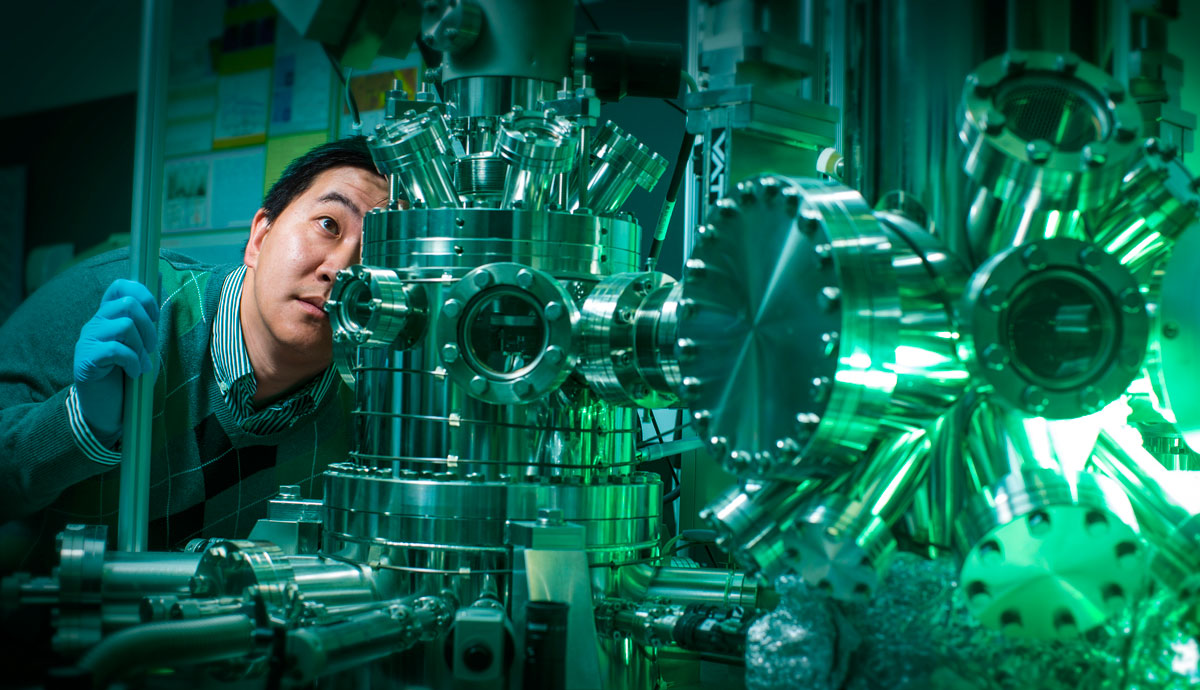
“When we vibrate the silicon atoms it causes heat and the atoms disassemble,” Dr Du said. “Then we use two small robotic arms that we move with a hand-held video game controller to catch the atoms in the vacuum chamber and place them one at a time on a plate to form the silicene paper.
“The process is like laying bricks, only these are bricks are the size of a single atom. A 1 centimetre-long chain contains 10 million silicon atoms.”
Studying the fundamental physics is helping the researchers build a more complete picture of the material, its properties and how to make it. The next step will be to integrate it into electronic devices and test its usefulness for specific applications.
“The challenge is to make large-scale and high-quality silicene layers that are large enough for integrated circuits,” Dr Du said. “There is also work to be done in developing ways to peel and transfer the silicene layers from the base it has been assembled on, as well as embed electrodes in it.”
He said the team, who along with their research collaborators in China, France, Germany and Italy are at the forefront of research and development into this new frontier material, were confident they will overcome these challenges.
The research findings have been published in recent months in the journals , and .
